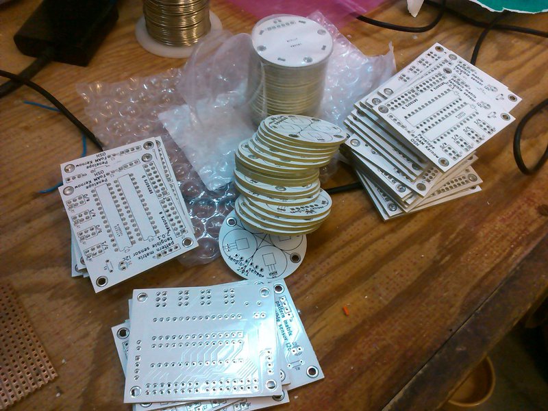
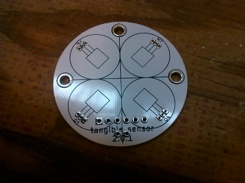
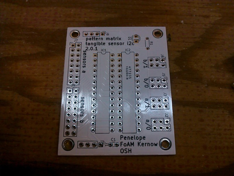
After triple checking the schematics and design files and ordering 80 PCBs (50 sensors and 30 i2c boards) there was an anxious wait for them to arrive and do some initial tests to find out if there were any mistakes. We now have enough boards to make two new pattern matrix devices, one 4X4 and one 5X5 - the plan is to evaluate the design and refine it for future builds.
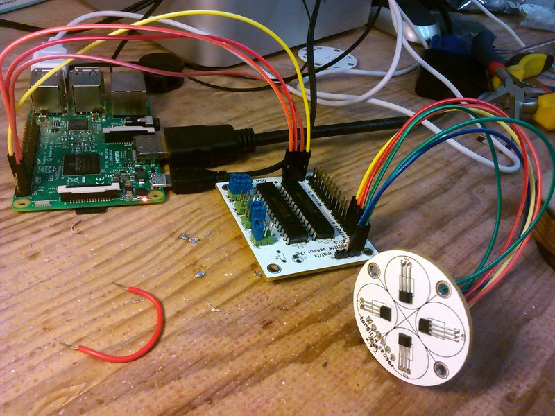
The picture below shows the first test boards populated and plugged it into the Pi - it's much neater than the lego and breadboard prototype! The good news is that it seems to work so far, the only problem I've had is with the hall effect sensors, the pads are a tiny bit too close together for my skills. After a couple of tricky situations fixed with a de-soldering pump, I think I've come up with a strategy that works. I can bend the outer pins away from each other and solder the central pin first - then bend them back to finish the outer ones and being very careful not to bridge the pads.
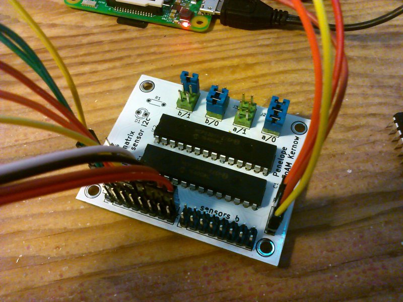
The blue jumpers on the square i2c boards allow you to program the device channel that the two expanders use - these could alternatively be hard soldered, but it's good to have the option to reuse the parts or reconfigure a pattern matrix so we can add different sensors etc.
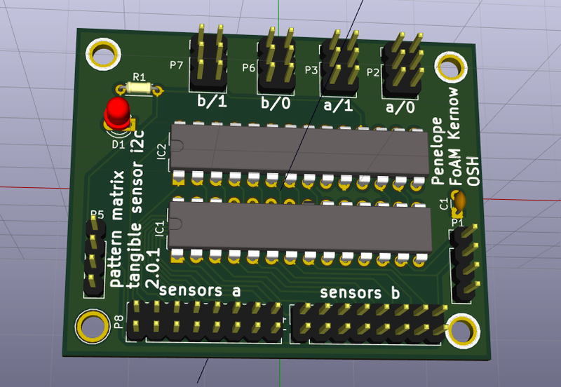
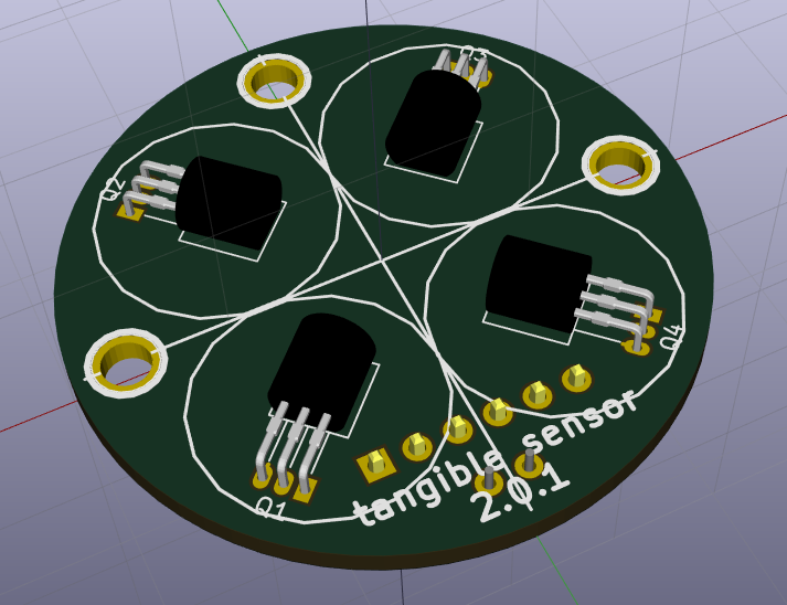
For reference, the KiCad 3D viewer models look pretty close.